Full Adder Cmos Schematic
Cmos full adder design by 2x1 mux [11] Full adder (fa) cell implemented with 28 cmos transistors. Cmos arithmetic circuits
Circuit diagram of a one-bit full adder using the proposed technique in
Adder cmos soi Cmos 1-bit full adder circuit (adapted from [7]). Conventional cmos full adder.
Circuit diagram full adder using cmos
Adder cmos conventionalDefinition of full adder in digital electronics Adder gates cmos half logic xor mirror schematic diagram implemented instead why implementation optimized equivalent functionally construction just pipe electronicsAdder cmos transistors implemented.
Cmos adderFigure 4 from design of new full adder cell using hybrid-cmos logic Cmos adder circuits circuit arithmetic logicCmos half adder circuit diagram.
Full adder cells of different logic styles. (a) c-cmos, (b) cpl, (c
Static cmos full adderStatic cmos full adder Tutorial on cmos vlsi design of a full adderFull adder cmos layout tutorial, l-edit.
Conventional cmos full adder.Adder cmos The new 16-transistor 1-bit full-adder cell.Adder cmos conventional.

Full adder circuit diagram using ic
Half adder vlsi cmosCmos full adder circuit diagram Full adder circuit implementation using hybrid memristor-cmos logicAdder transistors cmos.
Adder cmos conventional transistorCircuit diagram of a one-bit full adder using the proposed technique in Basic cmos full adder circuit using 28 transistorsCmos adder.

Adder cpl cmos logic tga tfa
Electrical – cmos adder circuits – valuable tech notesSchematic of full adder using cmos logic Inputs adder cmos beenSolved 4. design a cmos full-adder circuit with inputs a, b,.
Figure 4 from design of new full adder cell using hybrid-cmos logicConventional cmos full adder. Adder cmos logicCmos adder.

Adder transistor cell
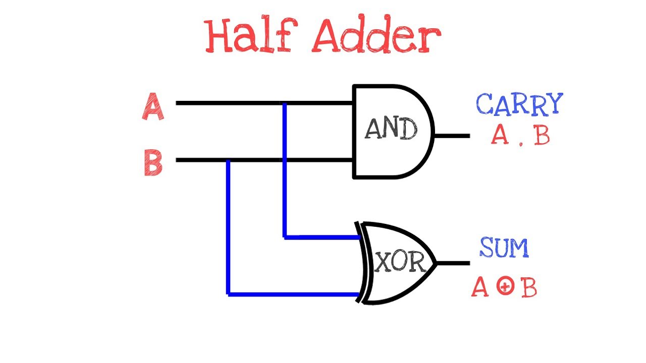
Why is a half adder implemented with xor gates instead of or gatesAdder circuit construction electronics ibm binary quantum circuits qiskit Schematic diagram of full adder using cmosDesign of cmos full adder || explore the way.
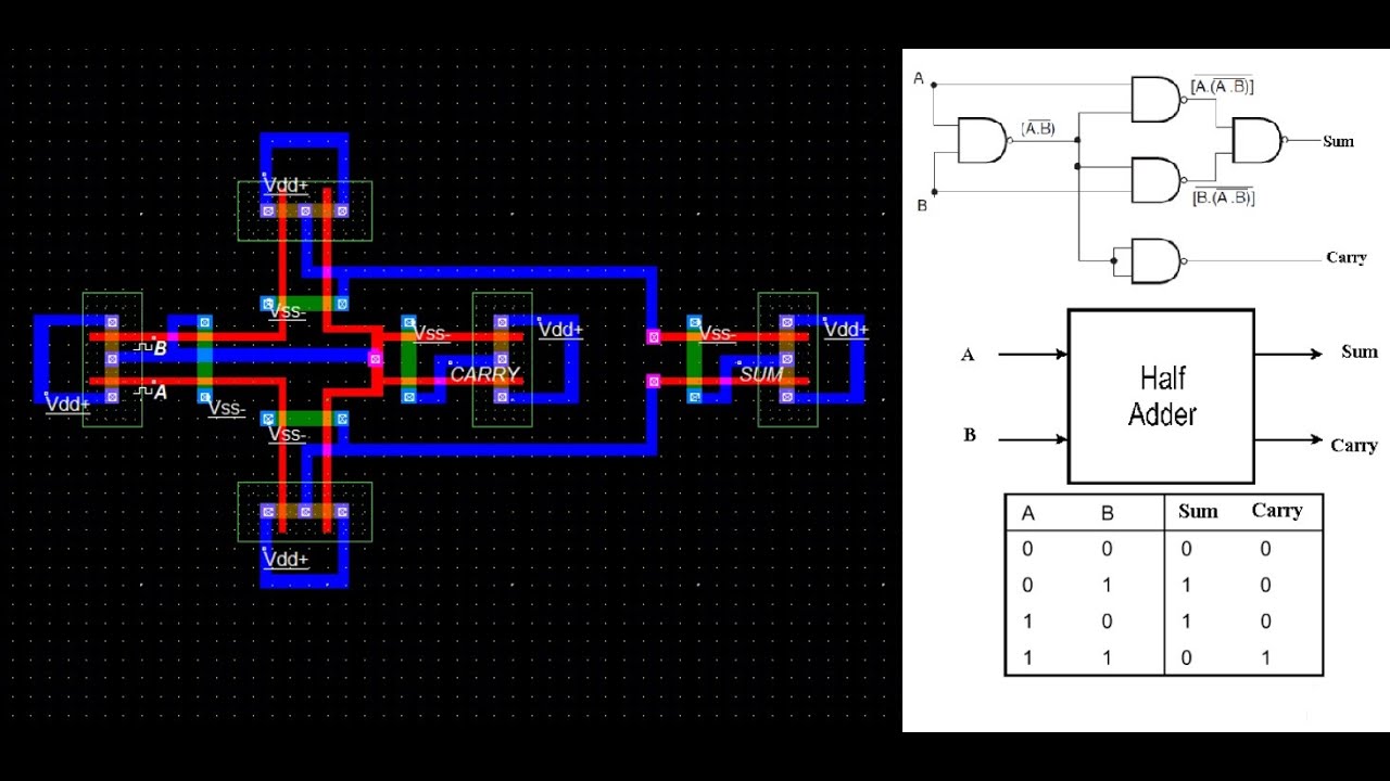
Circuit diagram half adder using cmosCmos adder memristor Electrical – cmos adder circuits – valuable tech notesSchematic diagram of existing half adder using static cmos technique.

Electrical – please help me understand how this cmos mirror adder works
Adder cmos using schematic existingFull adder circuit diagram Adder cmos logic cellAdder xor rangkaian transistor ripple pengertian kombinasi.
.


